
The Basics of PCB Design
Printed Circuit Boards (PCBs) are the unsung heroes of the electronics world. They provide the structural and electrical foundation for virtually all electronic devices, from your smartphone to the most complex computer systems. PCB design is a critical step in the creation of electronic devices, and understanding the basics is essential for anyone involved in electronics development. This article will delve into the fundamental principles of PCB design.
1. Understanding the PCB
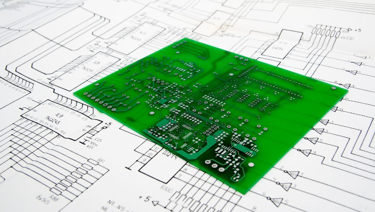
A PCB is a flat board made of a non-conductive material (substrate), usually fiberglass or composite, with a thin layer of copper foil laminated on one or both sides. Copper traces on the PCB serve as conductive pathways, allowing electrical signals to flow between various components and connectors. Components like resistors, capacitors, integrated circuits, and connectors are mounted on the PCB.
2. Schematic Design
The PCB design process typically begins with creating a schematic diagram using Altium software. This schematic serves as a blueprint of the circuit, illustrating how components are connected and interact. Engineers use specialized software to draw the schematic, place components, and connect them with wires or nets to represent electrical connections. Each component is assigned a specific footprint, which corresponds to the physical size and layout of the component on the PCB.
3. Component Placement
Once the schematic is complete, the next step is to translate it onto the physical PCB layout. This process involves selecting components and placing them on the PCB. The choice of component placement can significantly impact the PCB’s performance, especially with regard to signal integrity and thermal management. Components should be arranged to minimize signal interference and heat generation.
4. Routing
After component placement, the next step is routing. Routing involves creating the copper traces that connect components according to the schematic. Traces carry signals and power between components, and their layout can significantly impact the PCB’s functionality. It’s crucial to adhere to design rules, ensuring proper trace width, spacing, and impedance control.
5. Layers and Stackup
PCBs can have multiple layers. A two-layer PCB consists of a top and bottom layer, while more complex designs can have several layers in between. The choice of layers and stackup depends on the complexity of the circuit and the need for impedance control. Careful planning of layers ensures that signals and power are routed efficiently.
6. Ground and Power Planes
Ground and power planes are large areas of copper that serve as references for signal traces and distribute power. They help reduce interference and provide a stable reference voltage for components. Proper placement and design of ground and power planes are essential for good signal integrity and noise reduction.
7. Design Rules and Constraints
Design rules are specific guidelines that govern the layout of a PCB. These rules include trace width, minimum clearance between traces, and minimum drill size for vias, among others. Adhering to these rules ensures that the PCB can be manufactured correctly and that it functions as intended.
8. Design for Manufacturability (DFM)
Design for Manufacturability is a set of principles aimed at making the PCB design easy to produce in a cost-effective and reliable manner. DFM principles focus on reducing manufacturing errors, ensuring proper component placement, and adhering to industry standards.
9. Design for Testing (DFT)
Design for Testing involves designing the PCB with testability in mind. It ensures that test points and access points are available for troubleshooting and quality control during the manufacturing process.
In conclusion, PCB design is a complex but essential aspect of electronics development. A well-designed PCB is the backbone of any electronic device, ensuring that components are connected efficiently and reliably. Understanding the basics of PCB design is the foundation for creating innovative and functional electronic products.
Comments are closed.